
DIODES APPLICATIONS –SPECIAL PURPOSE DIODES
OBJECTIVES
INTRODUCTION
Semiconductors are materials which are used to manufacture all electronic and optoelectronic devices, computers components, IC’s (integrated circuits), mems (microelectromecahnical sytems) and even nanodevices (example quantum dot leds’ ) today. They are so widely used because of their special band gap and its related properties. They even differ from conductors and insulators in their electrical and optical properties because of their band gap (Eg) being different than that of conductors and insulators. Now band gap of a material is defined as the energy difference between conduction band and valence band in terms of electron energy. It is a major factor in deciding a material application for e.g. Conductors have no Eg, semiconductors have an Eg of the order of 1ev.

At room temperature, conductors have very high number of charge carriers in conduction band which gives high conductivity whereas for the case of insulators very few electrons reach the conduction band at room temperature. For semiconductors reasonable numbers of charge carriers reach the conduction band. Refer table 1.1. There is a direct relation between intrinsic charge carrier concentration (ni) and conductivities (σ). Since Ge has three orders of ni greater than that of Si therefore its conductivity (σ) is also 3 orders higher. It is to be noted that they are both good conductors at room temperature.
TABLE 3.1
|
Insulators |
Semiconductor |
Conductor |
|
Band Gap |
> 5 ev |
~ 1.1 |
~ 0.6 |
No band gap |
Resistivity (ρ) |
10 -12 |
0.02 |
0,02 x 10 -3 |
10 6 |
ni ( cm -3 ) |
--- |
1.5 x 10 10 |
2.5 x 10 13 |
~ 10 23 |
Temperature |
Positive |
Positive |
Positive |
Negative |
The resistance of conductors increases with increase in temperature because the lattice vibrations block the free flow of electrons on application of potential. For the case of intrinsic semiconductor the resistance decreases more electron hole pairs are generated because of breakage of bonds. With an addition of small amount of impurity (one in 10 7 atoms) from third group or fifth group , the conductivity increases by an order of 10 5 . This si because number of free charge carriers increases by 10 5 times ( 1012 / 107 ).
DIODES : FABRICATION AND CONSTRUCTION: A diode is a two terminal device made by a P type and n type materials or between a semiconductor and a metal. If the junction is made between a metal and semiconductor then it is called a Schottky diode whose application is in rectifying and non-rectifying contacts and Schottky devices.
There are various methods of fabrication of a junction depending on the application of the diode.
Table 3.2 gives selected a few techniques and applications.
S.N. |
Fabrication Technique |
Application |
1 |
Alloy Junction: A small dot of In is kept on n type Si and heated to 150oC. It melts and dissolves. The temperature is then lowered. |
High |
2. |
Point Contact: The junction area is kept very small so that the capacitance value is low. |
High |
3. |
Epitaxial Growth: Junction is fabricated on an epitaxial layer. |
Low |
4. |
Grown Junction: Czochralski technique where a single semiconductor seed which is immersed in molten semiconductor material is gradually with drawn with the help of a rod which holds the seed. pn junction is fabricated by first adding p type and then n type impurity. |
High current application because of high area of contact. |
When the pn junction is made, there is a transfer of charge through the junction region because of concentration gradient of the charge carriers, as shown in fig 1.2. This creates a barrier potential.) The direction of barrier potential is as shown by the arrow from n type to p type. It is the formation of potential barrier that makes the device useful since it can be controlled by various factors like biasing etc.
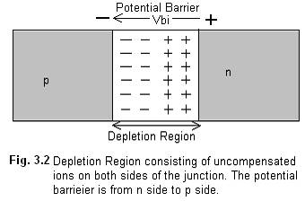
The direction of this field is from n side to p side as shown in figure 2. The equation of this field barrier (Vbi) is given by

where Na and Nd are the acceptor and donor concentrations, ni is the intrinsic concentration, q is the electron charge and T is the temperature in absolute values. Vbi
is lesser for Ge ( 0.2 V ) than for Si (0.6 V ) since ni is higher for Ge compared to Si.
If a voltage V is applied across the diode, the current flowing across it is given by the Shockley equation

where V is the bias potential across the diode. The factor h is 1 for Si and 2 for Ge diodes. Vt is volt equivalent of temperature and is given by 11,600 / T. Its value at room temperature is 26 mV. Io is the reverse saturation current in mA which depends upon temperature and doping. This is called reverse saturation since its value cannot be increased by increasing Vr.
Forward Biasing: If an external voltage is applied such that negative of battery is connected to n side and positive to the p side then Vbi will get reduced and more current can flow across the junction. Reverse Bias On the other hand if an external voltage is applied in the reverse direction i.e. positive of battery to n side and negative of battery to p side then the barrier potential increases and only minority charge carriers flow across the junction. Thus the current is very small in microamperes and is independent of the external voltage, up to a certain voltage. Beyond this voltage, the diode breaks down by either Avalanche breakdown mechanism or Zener breakdown mechanism.
PEAK INVERSE VOLTAGE (PIV):
PIV is the maximum reverse bias voltage which can be applied safely to a diode without its breaking down. Beyond this voltage a diode breaks down.
Avalanche Breakdown The minority carriers which are diffusing across the junction get sufficient energy from the increased voltage to break the covalent bonds and generate more Electron hole pairs. These generated pairs break more bonds and this process is multiplicative. Thus at the breakdown condition the current suddenly shoots up because of additional extra pairs.
ZENER breakdown This is applicable only to heavily doped junctions which have a very narrow depletion layer. On increase of reverse voltage the electric field increases so much that the covalent bonds break and generate minority carriers which constitute the reverse current.
One can know whether a specific terminal of a diode is n or p by measuring the resistance with multimeter. To do so keep the multimeters in resistance mode connect its positive lead to the anode of diode and negative lead to its cathode. During the test ,the multimeter passes current through the diode and the diode gets forward biased. It thus indicated very low resistance of the order of 100 W . If the leads are now reversed than the diode gets reverse biased and offers very high resistance of the order of MW. This can be read in the multimeter again. If a diode reads very low resistance in the forward as well as reverse bias then it is fused. On the other hand if it reads high resistance in the forward as well as reverse bias then it is open.
Table 3.1 gives the comparison of Si and Ge diodes in terms of band gap (Eg) Vbi and, PIV
TABLE 3.1.
Diode Material |
Eg |
Vbi |
PIV |
Ge Diode |
0.785 |
0.2 |
400 |
Si Diode |
1.21 |
0.6 |
1000 |
It is clear that Si diodes have an advantage over Ge diodes since their band gap is more and they have a higher PIV. If the band gap is more they are more impervious to temperature changes since there is a direct relation between Eg and working temperature. But Ge diodes are more useful for switching circuits since their Vbi is almost 0 V.
Table1.2 gives the specifications of some commonly used diodes.
TABLE 3.2 (edit to data sheet at end)
Device Number |
Material used. |
IF (mA) |
VF(V) |
VBR |
Power Rating (mW) |
OA91 |
Ge |
50 |
2.1 |
115 |
|
In 4148 |
Si |
100 |
1.0 |
75 |
|
In 4149 |
Si |
100 |
1.0 |
75 |
|
IN 4007 |
Si |
1000 |
1.6 |
1000 |
|
IN463 |
|
1.0 |
1.0 |
200 |
|
IN462 |
|
5.0 |
1.0 |
70 |
|
IN459A |
|
100.0 |
1.0 |
200 |
|
T151 |
|
200.0 |
1.0 |
20 |
|
BZX 88 series |
zener |
|
|
|
|
BZX85 |
zener |
|
|
|
|
3.1 AIM (a) To study the current – voltage characteristics of (i) Normal diode and (ii) Zener diode. Also to determine whether the given diode is Ge or Si diode with the help of characteristics
(b) To calculate its static and dynamic resistances.
APPARATUS AND COMPONENTS
Diode (IN 4148), Resistor (1K), bread board, single strand wires, DC Power supply (~ 0-20V), Digital Multimeters (2) or Voltmeters (~ 0-5V for forward bias and ~ 0-20V for reverse Bias), Ammeter (~0-20mA for forward bias and 100 μa for reverse bias).
THEORY
A diode is defined to have two kinds of resistances – Static resistance (rdc ) and AC dynamic resistance. (rac) The static resistance is given by the ratio of dc voltage across a diode to the dc current. This can be determined from the dc characteristic curve and is not constant and varies with forward bias. Depending upon the operating point its value could vary from 0.05 W to 250 W . For Reverse bias, rdc is 5M W. Dynamic resistanceis the resistance offered by a diode to an ac signal. Since the slope of the curve at a particular voltage is given by DIF / DVF hence rac at that voltage is the reciprocal of the slope. (rac =DVF / D IF). Its range is generally in 1 to 25 ohms and its value is determined by the shape of the curve at that point.
To plot the forward bias characteristics, do the connections as in fig. 3.1.1. Apply forward bias from 1 V to 2 V in steps of 0.1 V, note down the corresponding current readings and tabulate as in table 3.1.1. For reverse bias do the connections as in fig. 3.1.2 and apply reverse bias from 0V to 20 V in steps of 1 V. Tabulate the readings as in table 3.1.2. Note the current in reverse bias is due to minority carriers only hence its magnitude is in microamperes only.

CALCULATIONS AND RESULTS:
Forward characteristics and reverse characteristics have been plotted in Fig. 3.1.3 and 3.1.4 respectively. It is noted that since the cut in voltage is approximately 1 V hence it is a Si diode and not a Ge diode. The Rdc and Rac are calculated as follows:
APPARATUS AND COMPONENTS
Diode (IN 4148), zener diode, Resistor (1K), bread board, single strand wires, function generator, CRO.
THEORY To observe current voltage characteristics directly on a CRO, the CRO has to be operated in X-Y mode. In this mode of operation the time base circuit of the CRO (i.e. which generates the saw tooth waveform) which is otherwise fed to the horizontal deflection system is replaced by the external signal on channel 2 of the CRO. So channel 1 is plotted on Y axis and channel 2 is plotted on the X axis. Hence for example if the 2 channels receive sine waves then lissajous figures (see chapter III) are plotted because the two sine waves superimpose at right angles on each other. On the other hand if channel 2 is connected across the resistor in the diode circuit, then current values of the circuit can be calculated as I = V / R. Now if channel 1 reads the voltage across the diode then I-V plots will be observed on the CRO.

3.3 AIM To study various clipping circuits.
APPARATUS Diode (IN 4148), Resistor (1K), bread board, single strand wires, Audio Oscillator, CRO.
THEORY
DIODE CLIPPER (LIMITER) AND CLAMPER
Clippers are those circuits, which have the ability to clip off some portion of the alternating waveform, with the rest of the waveform remaining the same. They are also known as limiters. There are two types of clippers: Series clippers (i.e. when the diode is in series with the load) and parallel clippers (diode is in parallel with the load). Half wave rectifiers are examples of clippers since they clip off negative half of the waveform.
SERIES CLIPPER: Can be divided into two classes - Positive clipper and Negative clipper.
Positive Clipper: In fig 3.3.1, an ac voltage applied to a diode in series with a load. During the positive half cycle of the sine wave the diode is reverse biased hence it is cut off and no current flows in the circuit. Therefore the output is zero. During the negative half cycle, diode is forward biased and 0.6 V appears across it. The rest of the voltage appears across the load therefore the output is 0.6 volts lesser than the input.

BIASED POSITIVE SERIES CLIPPER:
Refer Fig. 3.3.2. The n terminal of diode is given negative V voltage hence diode will refer V volts as it’s reference (ground) level and output will oscillate around V volts. During the positive half cycle it will conduct till V voltage after which it is cut off. During negative half cycle it is forward biased hence it conducts fully and the output will be greater than V volts than the input.

In fig. 3.3.3, the n junction of the diode is given a positive (reverse ) bias of V volts hence the output will oscillate around V volts. During the positive half cycle it does not conduct at all and during the negative half cycle it only starts conducting after V volts.

NEGATIVE CLIPPER In fig 3.3.4, negative half of the ac input is clipped off because of the diode’s configuration as shown. If a negative V volt is applied to the anode of diode then it will be reverse biased by V volts. On application of ac voltage it will only conduct for voltages above V volts as shown in fig. 3.3.5 In fig 3.3.6, the battery has been reversed so that the diode is forward biased by V volt. Hence in the negative half cycle, it is forward biased till –V volts and will only stop conduction after V volts. This is called biased negative clipper.


PARALLEL CLIPPER Parallel clippers can be divided into two classes: Positive parallel and negative parallel clippers.
PARALLEL POSITIVE CLIPPER In fig. 3.3.7, since the diode is in parallel with the input and output hence it is called as parallel clipper. During the positive half cycle, the diode conducts and the output voltage is 0.7 V. In the negative half cycle, it acts as a high resistor. 
Hence output follows the input. Fig 3.3.8 shows a biased clipper where the diode is reverse biased by V volt. In the positive half cycle it only starts conducting for voltage above V volts. Hence the circuit is clipped above V volts where the output is shorted. For input less than V volt, the diode is reverse biased and offers high resistance. Therefore output follows input. If the polarity of battery is reversed as in fig. 1.21, then diode is forward biased by V volt. It offers high impedance only for voltages below -V volt In fig. 1.21 the diode does not conduct for positive half cycle hence the output follows the input.


In fig 3.3.10, during the negative half cycle, the diode conducts and the output voltage is 0.7 V. In the positive half cycle, it acts as a high resistor. Hence output follows the input. If a battery is added to this circuit so as to reverse bias the diode as in fig. 3.3.11, then the diode offers high resistance till –V volt and output follows the input till –V volt. On the other hand if the polarity of diode is reversed then it conducts in positive half cycle below V volt and output is V volt, as shown in fig. 3.3.12.

In fig 3.3.13, two diodes have been added in parallel with the load. Diode D1 is reverse biased by V1 volt and diode D2 is reverse biased by V2 volt. During positive half cycle, D1 conducts only above V1 volt and D2 offer high impedance. Hence output is same as input below V1 volt for positive half cycle. During the negative half cycle, , D2 conducts only below –V2 and D1 offers high impedance. Therefore output follows input above –V2 volt during negative half cycle.

In fig. 3.3.14, the output follows the input only in between the voltage levels V1 and V2 where V2 is less than V1. Diodes D1 and D2 are in parallel with the output and D1 is forward biased by V1 and D2 is reversed biased by V2. When Vin is less than V1, D1 is forward biased and D2 is off. The output is equal to V1. When Vin is greater than V1 and less than V2, both D1 D2 are reverse biased. Then the output follows the input. For voltages above V2, D1 is off and D2 conducts. Therefore output is equal to V2.
PROCEDURE
Do the connections as in fig. 3.3.1. Connect the CRO across the output. Apply sine wave of suitable frequency and voltage greater than 4 V peak to peak. Trace the output on trace paper and note down its frequency. It is observed that the output wave is clipped on the positive half of cycle. Repeat this procedure for all circuits of figs 3.3.2 to 3.3.14.
One can also repeat this experiment using square waveform as the input.
Note down the difference of outputs from positive series clipper and positive parallel clipper.
RESULTS
The clipped waveforms of various circuits are as plotted on the output waveform side. In our case positive clipper output, the clipping does not start from 0 volts exactly. The reason is that the Si diode is reverse biased till 1 V approximately. Hence output voltage follows the input voltage till +1 V. If Ge diode is used instead then the output would be than that for the case of Si diode circuits. Similarly in case of negative clippers the output is not exactly a totally clipped waveform on the negative side. The reason is same as above.
3.4 AIM To study the positive Clamping and negative clamping circuits using diodes.
APPARATUS Diodes (In4148), Resistors (1K), Variable DC power supply, Audio Oscillator and CRO.
THEORY Clampers are circuits which change the reference voltage of an ac waveform. Alternatively, clampers are also said to be those circuits which add a dc level to an ac waveform. The essential components are a capacitor, a diode and a resistor. Positive Clamper: Consider Fig. 3.4.1. During the negative half cycle, the diode conducts and the capacitor charges to V volts as shown. In the positive half cycle, the capacitor which was charged initially, discharges through the resistor by time constant RC. This happens only if RC time constant is much less than half the time period of the waveform. Hence if RC is larger than half the time period, it will not discharge through R. Now C acts as a battery of V1 volt. Hence during the positive half cycle, the diode is reverse biased by (input + V1) volts, which appears across it.

Biased Positive Clamper: Biased clamper circuits produce an output waveform which is clamped by a variable level defined by the biasing voltage of the diode. If a battery of value V2 is added to forward bias the diode of fig. 3.4.1 then the clamping level of the output waveform is raised from V1 to V1 + V2 volts. Consider fig. 3.4.2, where during negative cycle the output voltage is V2 volts. The capacitor gets charged to V1 + V2 volts. In the positive half cycle the same C acts as a battery of V1 +V2 volts hence the output is ( 2 x I/P + V2 ) volts.

Fig. 3.4.3 is a circuit where the output is –V2 during negative half cycle and C is charged to (V1 – V2 ) volts. Therefore during positive half cycle the output is ( 2x Input – V2 ) volts.

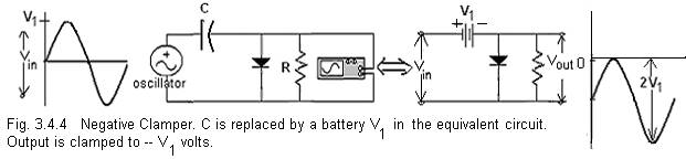
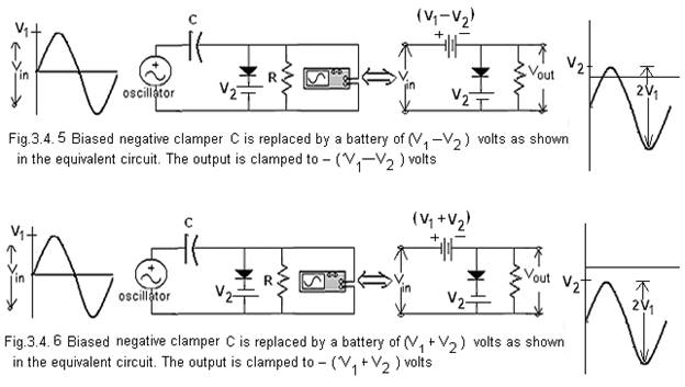
Negative Clampers: These circuits clamp the waveform to some negative level which is decided by the peak input voltage and the biasing battery. In fig 3.4.4, the output has been clamped to –V1 volts. If a battery of V2 volt is added as shown in fig 3.4.5 then the output is clamped to (-V1 + V2) volts. Similarly is figure 3.4.5 the output is clamped to (-V1 - V2) volts. In case of negative clampers the capacitor gets charged in the opposite direction of that of positive clampers.
PROCEDURE
Do the connections as in circuit 3.4.1. Connect the CRO across R. Apply ac waveform of suitable frequency to the input terminal and trace the output from CRO. Repeat the same procedure for circuits from 3.4.2 to 3.4.5.
RESULTS The clamped waveforms of various circuits are as plotted on the output waveform side of the respective circuits.
PRECAUTIONS
3.5 AIM To study voltage multiplier circuits.
APPARATUS Diodes (In4148), Variable DC power supply, Audio Oscillator and CRO.
THEORY Voltage multipliers are circuits which can convert an ac waveform into an amplified dc voltage. Essential components are capacitors and diodes. Fig. 3.5.1 is a circuit of half wave voltage multipliers.. Circuit (a) is that of a doubler which can be divided into 2 stages: A negative clamper exhibited by C1 and D1, followed by a half wave rectifier and a filter circuit consisting of C2 and D2. Fig (b) shows that during positive half cycle, C1 charges to V1. and D1 is a short. In fig (c), during the negative half cycle, C1 acts as a battery of V1 volts, D1 is non conducting, D2 conducts and C2 charges to 2V1.

Fig (d) is that of an n stage voltage multiplier, where voltage is multiplied 2n timed the input peak voltage. Output voltage is 2nV1 where V1 is input peak voltage.
A full wave voltage multiplier is shown in fig. 3.5.2. During the positive half cycle, D2 does not conduct, D1 conducts and C1 charges to V1. During negative half cycle, D1 does not conduct, D2 conducts and output across C1 and C2 is 2V1. Also the output is of full wave rectifier and since it is across 2 capacitor in series hence filtering is poorer as compared to the case when the output is across 1 capacitor.
Questions
With the help of load line, one can determine the operating point of a device and also the values of instantaneous voltages and currents across the device. If the load resistance is RL then by applying KVL to the circuit of fig. 1.10, one can write
![]()
where I is the current, vd is the voltage across diode and vi is the input voltage. For I = 0 , vd = vi and for vd = 0, I = vi / RL. Mark these points on the corresponding axis and draw a straight line through them as in fig. 1.11. The point of intersection of the straight line with the static curve gives the current that will flow under the given conditions. This also called Q point or operating point.

Diode Applications:
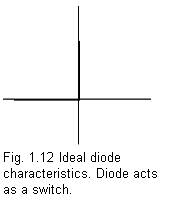
Ideal Diode If the diodes acts as perfect conductor (no voltage drop) in forward bias and perfect insulator (no current ) in reverse bias, then it is called an ideal diode. This can also be called as a switch. The Characteristics are shown in fig. 1.12.

Source: http://people.du.ac.in/~snagpal/part1_chap3_diodes.doc
Web site to visit: http://people.du.ac.in
Author of the text: indicated on the source document of the above text
If you are the author of the text above and you not agree to share your knowledge for teaching, research, scholarship (for fair use as indicated in the United States copyrigh low) please send us an e-mail and we will remove your text quickly. Fair use is a limitation and exception to the exclusive right granted by copyright law to the author of a creative work. In United States copyright law, fair use is a doctrine that permits limited use of copyrighted material without acquiring permission from the rights holders. Examples of fair use include commentary, search engines, criticism, news reporting, research, teaching, library archiving and scholarship. It provides for the legal, unlicensed citation or incorporation of copyrighted material in another author's work under a four-factor balancing test. (source: http://en.wikipedia.org/wiki/Fair_use)
The information of medicine and health contained in the site are of a general nature and purpose which is purely informative and for this reason may not replace in any case, the council of a doctor or a qualified entity legally to the profession.
The texts are the property of their respective authors and we thank them for giving us the opportunity to share for free to students, teachers and users of the Web their texts will used only for illustrative educational and scientific purposes only.
All the information in our site are given for nonprofit educational purposes