
1. What are the different fabrication processes available to CMOS technology?
a. p-well process
b. n-well process
c. Twin-tub process
d. Silicon On Insulator (SOI) / Silicon On Sapphire (SOS) process
2. What is intrinsic and extrinsic semiconductor?
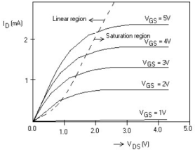
The pure silicon is known as Intrinsic Semiconductor. When impurity is added with pure silicon, it is electrical properties are varied. This is known as Extrinsic semiconductor.
3. What are the steps involved in manufacturing of IC?
`` i. wafer preparation
ii. Epitaxial growth
iii. Oxidation
iv. photo lithography
v. Diffusion and Ion Implantation
vi. Isolation
vii. Metallization
4. What is meant by ‘ epitaxy ’ ?
Epitaxy means arranging atoms in single crystal fashion upon a single crystal substrate.
5. What are the processes involved in photo lithography?
i. making process
ii. photo etching process
these are important process involved in photolithography.
6. What is the purpose of masking in fabrication of IC?
Masking is used to identify the place in which Ion Implantion should not be occurred.
7. What are the materials used for masking?
Photo resist, Sio2, SiN, poly Silicon.
8. What are the types of etching?
Wet etching and dry etching are the types of photo etching.
9. What is diffusion process? What are doping impurities?
Diffusion is a process in which impurities are diffused in to the silicon chip at 10000C temperature. B2O3 and P2O5 are used as impurities.
10. What is isolation?
It is a process used to provide electrical isolation between different components and interconnections.
11. What are the various CMOS technologies?
Various CMOS technologies are
12. What is channel stop implantation?
In n-well fabrication, n-well is protected with resist material. Because, it should not be affected by Boron implantation. The boron is implanexcept n-well. It is done using photoresist mask. This type of implantation is known as channel implantation.
13. What is twin-tub process? Why it is called so?
Twin-tub process is one of the CMOS technologies. There are two wells are available in this process. The other name of well is tub. So, because of these two tubs, this process is known as twin-tub process.
14. What is the special feature of twin-tub process?
In twin-tub process, threshold voltage, body effect n and p devices are independently optimized.
15. What are the advantages of twin-tub process?
Advantages of twin-tub process are
16. What is SOI? What is the material used as Insulator?
SOI means Silicon-on-Insulator. In this process, Sapphire or SiO2 is used as insulator.
17. What are the various etching process used in SOI process?
Various etching process used in SOI are
18. What are the advantages and disadvantages 0f SOI process?
Advantages of SOI process
Disadvantages of SOI process
19. What are BiCMOS Gates?
When bipolar and MOS technology are merged, the resulting circuits are referred to as biCMOS circuits. High gain vertical npn transistors with their collectors tied to the positive rail, and medium-gain lateral npn transistors are both compatible with conventional CMOS processing. BiCMOS gates can be used to improve the performance of line drivers and sense amplifiers.
20. Compare between CMOS and bipolar technologies.

UNIT –II BASIC ELECTRICAL PROPERTIES OF MOS CIRCUITS
1. Define Threshold voltage
The threshold voltage VT for a MOS transistor can be defined as the
voltage between the gate and the source terminals below which the drain
to source current effectively drops to zero.
2. Define body effect or substrate bias effect.
The threshold voltage VT is not a constant with respect to the voltage
difference between the substrate and the source of the MOS transistor.
This effect is called the body effect or substrate bias effect.
3. Give the different modes of operation of MOS transistor
Cut off mode
Linear mode
Saturation mode
4. What are the different regions of operation of a MOS transistor?
a. Cut off region
Here the current flow is essentially zero (accumulation mode)
b. Linear region
It is also called weak inversion region where the drain current is
dependent on the gate and the drain voltage w. r. to the substrate.
c. Saturation region
Channel is strongly inverted and the drain current flow is ideally
independent of the drain-source voltage (strong-inversion region).
5. Give the expressions for drain current for different modes of operation of
MOS transistor.
a. Cut off region
ID =0
b. Linear region
ID = kn [(VGS – VT) VDS – VDS2/2]
c. Saturation region
ID = (kn /2) (VGS – VT)2
6. Plot the current-voltage characteristics of a nMOS transistor.
7. Define accumulation mode.
The initial distribution of mobile positive holes in a p type silicon substrate of a mos transistor for a voltage much less than the threshold voltage
8. What are the secondary effects of MOS transistor?
a. Threshold voltage variations
b. Source to drain resistance
c. Variation in I-V characteristics
d. Subthreshold conduction
e. CMOS latchup
9. What is CMOS latchup?
The MOS technology contains a number of intrinsic bipolar transistors.These are especially troublesome in CMOS processes, where the combination of wells and subtrates results in the formation of p-n-p-n structures. Triggering these thyristor like devices leads to a shorting of VDD & VSS lines, usually resulting in a destruction of the chip.
10. What are the remedies to prevent Latch-up?
The remedies for the latch-up problem include:
(i) an increase in substrate doping levels with a consequent drop in the value of Rpsubs.
(ii) reducing Rnwell by control of fabrication parameters and ensuring a low contact resistance to VDD.
(iii) by introducing guard rings.
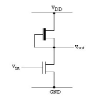
10. Draw the circuit of a nMOS inverter.
. 
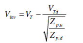
11. Give the expression for pull-up to pull-down ratio ( Zpu/Zpd) for an nMOS inverter driven by another nMOS inverter.
. 
12. Draw the circuit of a CMOS inverter.

13. What are the advantages of CMOS inverter over the other inverter
configurations?
a. The steady state power dissipation of the CMOS inverter circuit is
negligible.
b. The voltage transfer characteristic (VTC) exhibits a full output voltage wing between 0V and VDD. This results in high noise margin.
14. what are the possible modes in nMOS enhancement transistor?
i. accumulation mode
ii. depletion mode
ii. Inversion mode
15. In saturation region, what are the factors that affect Ids?
i. distancebetween source and drain.
ii. channel width
iii.Threshold oltage
iv.thickness of oxide layer
v. dielectric constant of gate insulator
vi. Carrier mobility.
16. What is Body effect?
The threshold voltage VT is not a constant w. r. to the voltage difference between the substrate and the source of MOS transistor. This effect is called substrate-bias effect or body effect.
17.What is Channel-length modulation?
The current between drain and source terminals is constant and independent of the applied voltage over the terminals. This is not entirely correct. The effective length of the conductive channel is actually modulated by the applied VDS, increasing VDS causes the depletion region at the drain junction to grow, reducing the length of the effective channel.
18.Define Threshold voltage in CMOS?
The Threshold voltage, VT for a MOS transistor can be defined as the voltage applied between the gate and the source of the MOS transistor below which the drain to source current, IDS effectively drops to zero.
19.What is pull down device?
A device connected so as to pull the output voltage to the lower supply voltage usually 0V is called pull down device.
20.What is pull up device?
A device connected so as to pull the output voltage to the upper supply voltage usually VDD is called pull up device.
21. Why NMOS technology is preferred more than PMOS technology?
N- channel transistors has greater switching speed when compared tp PMOS transistors.
22. What are the different operating regions of an MOS transistor?
Cutoff region
Non- Saturated Region
Saturated Region
UNIT – III - MOS CIRCUIT CONCEPT AND DESIGN PROCESS
1. What are stick diagrams?
Stick diagrams are used to convey layer information through the
use of a color code. A stick diagram is a cartoon of a chip layout. They
are not exact models of layout. The stick diagram represents the
rectangles with lines which represent wires and component symbols.
2. What are the different color codes used for single poly silicon nMOS
technology?
n-diffusion (n-diff.) and other thinoxide regions -green
Polysilicon (poly.) - red
Metal 1 (metal) - blue
Implant - yellow
Contacts - black or brown (buried)
3. What are design rules?
Design rules are the communication link between the designer specifying requirements and the fabricator who materializes them. Design rules are used to produce workable mask layouts from which the various layers in silicon will be formed or patterned.
4. Define Rise time
Rise time, tr is the time taken for a waveform to rise from 10% to 90% of its steady-state value.
5. Define Fall time
Fall time, tf is the time taken for a waveform to fall from 90% to 10% of its steady-state value.
6. Define Delay time
Delay time, td is the time difference between input transition (50%) and the 50% output level. This is the time taken for a logic transition to pass from input to output.
7. What are two components of Power dissipation.
There are two components that establish the amount of power dissipated in a
CMOS circuit. These are:
i) Static dissipation due to leakage current or other current drawn continuously from the power supply.
ii) Dynamic dissipation due to
- Switching transient current
- Charging and discharging of load capacitances.
8. What is meant by interconnect? What are the types of interconnect?
Interconnect means connection between various components in an IC
Types of Interconnect
Metal Interconnect
Polysilicon Inter connect.
Local Inter Connect.
9. What is silicide?
The combination of Silicon and tantalum is known as Silicide. It is used as gate materials
in polysilicon interconnect.
10. What are the two types of Layout design rules?
Lambda (λ) design rules and micron rules are major types of layout design rules.
11. Write the Significance of Sheet resistance
As the line width becomes smaller, sheet resistance contributes to the RC delay increase.
12. List the processes used for deposition of metals prior to sintering while using silicide for polysilicon.
1. Sputtering or evaporation
2. Co-sputtering metal and silicon in the desired ration from two independent targets
3. co-evaporation from the elements
13. Define Delay time
Delay time, td is the time difference between input transition (50%) and the 50% output level. This is the time taken for a logic transition to pass from input to output.
14. Define a superbuffer.
A superbuffer is a symmetric inverting or noninverting gate that can
supply or remove large currents and switch large capacitive loads faster
than a standard inverter.
15.What are BiCMOS Gates?
When bipolar and MOS technology are merged, the resulting circuits are referred to as biCMOS circuits. High gain vertical npn transistors with their collectors tied to the positive rail, and medium-gain lateral npn transistors are both compatible with conventional CMOS processing. BiCMOS gates can be used to improve the performance of line drivers and sense amplifiers.
UNIT – IV - COMBINATIONAL AND SEQUENTIAL CIRCUIT DESIGN
1. What are the static properties of complementary CMOS Gates?
a. They exhibit rails-to-rail swing with VOH = VDD and VOL = GND.
b. The circuits have no static power dissipation, since the circuits are
designed such that the pull-down and pull-up networks are mutually exclusive.
c. The analysis of the DC voltage transfer characteristics and the noise
margins is more complicated than for the inverter, as these parameters depend upon the data input patterns applied to the gate.
2. Draw the equivalent RC model for a two-input NAND gate.

3. What are the major limitations associated with complementary CMOS gate?
a. The number of transistors required to implement an N fan-in gate is
2N. This can result in a significantly large implementation area.
b. The propagation delay of a complementary CMOS gate deteriorates
rapidly as a function of the fan-in.
4. What is meant by ratioed logic?
In ratioed logic, a gate consists of an nMOS pull-down network that
realizes the logic function and a simple load device, which replace the entire pull-up network. A ratioed logic which uses a grounded pMOS load is referred to as a pseudo-nMOS gate
5. What is true single phase clocked register?
The True single-phase clocked register (TSPCR) uses a single clock, CLK. For the positive latch, when CLK is high, the latch is in the transparent mode and corresponds to two cascaded inverters; the latch is non-inverting, and propagates the input to the output. On the other hand, when CLK=0, both inverters are disabled, and the latch is in the hold mode.
6. Define a tally circuit.
A tally circuit counts the number of inputs that are high and outputs the
answer. If there are N inputs there are N +1 possible outputs, corresponding
to 0, 1, 2, …. N inputs that are high.
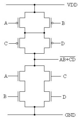
7. Implement y= (AB+CD)’ using CMOS logic
8. Draw the CMOS implementation of 4-to-1 MUX using transmission
gates .

9.What are the two types of MOSFET?
Two types of MOSET are n-channel MOSET and p-channel MOSFET. These are known as n-MOS and p-MOS.
10.which MOS can pass logic 1 and logic 0 strongly?
p-MOS can pass strong logic 1
n-MOS can pass strong logic 0
11. What is AOI logic function?
AND OR Invert logic function (AOI) implements operation in the order of AND, OR, NOT operations. So this logic function is known as AOI logic function.
12. What is bubble pushing?
According to De Morgan’s laws,
![]() =
= ![]() +
+![]()
![]() +
+![]() =
= ![]()
So NAND gate may be drawn as bubbled OR gate. Bubbles are introduced in the input side. This concept is known as bubble pushing.
13. Implement y = ![]() using bubble pushing concept?
using bubble pushing concept?
Y = ![]() can be implemented using bubbled AND gate.
can be implemented using bubbled AND gate.
![]() =
= ![]() +
+![]()
14. What is OAI 221 Gate?
OAI 221, here 221 refers to number of inputs in each section.
15. Write the features of CMOS Domino Logic?
16. What are the tally circuits?
17. What are the various forms of inverter based CMOS logic?
18. Differentiate between channeled & channel less gate array.
Channeled Gate Array Channel less Gate Array
1. Only the interconnect is customized only the top few mask layers are customized.
2. The interconnect uses predefined spaces between rows of base cells. No predefined areas are set aside for routing between cells.
3. Routing is done using the spaces Routing is done using the area of transistors unused.
4. Logic density is less Logic density is higher.
19. What are the different methods of programming of PALs?
The programming of PALs is done in three main ways:
• Fusible links
• UV – erasable EPROM
• EEPROM (E2PROM) – Electrically Erasable Programmable ROM
20.What is an antifuse?
An antifuse is normally high resistance (>100MW). On application of appropriate programming voltages, the antifuse is changed permanently to a low-resistance structure (200-500W).
21.What are macros?
The logic cells in a gate-array library are often called macros.
22. What are Programmable Interconnects?
In a PAL, the device is programmed by changing the characteristics if the switching element. An alternative would be to program the routing.
UNIT – V DESIGNING ARITHMETIC BUILDING BLOCKS
1. Give some of the important CAD tools.
Some of the important CAD tools are:
i) Layout editors
ii) Design Rule checkers (DRC)
iii) Circuit extraction
2.What is Verilog?
Verilog is a general purpose hardware descriptor language. It is similar in syntax to the C programming language. It can be used to model a digital system at many levels of abstraction ranging from the algorithmic level to the switch level.
3. What are the various modeling used in Verilog?
1. Gate-level modeling
2. Data-flow modeling
3. Switch-level modeling
4. Behavioral modeling
4. What is the structural gate-level modeling?
Structural modeling describes a digital logic networks in terms of the components that make up the system. Gate-level modeling is based on using primitive logic gates and specifying how they are wired together.
5.What is Switch-level modeling?
Verilog allows switch-level modeling that is based on the behavior of MOSFETs. Digital circuits at the MOS-transistor level are described using the MOSFET switches.
6. What are the types of programmable device?
Programmable logic structure
Programmable Interconnect
Reprogrammable gate arry
7. What is CLB?
CLB means Configurable Logic Block.
8. What are the advantages and disadvantages of PLA?
Advantages of PLA
Disadvantages of PLA
9. What is meant by FPGA?
A field programmable gate array (FPGA) is a programmable logic device that supports implementation of relatively large logic circuits. FPGAs can be used to implement a logic circuit with more than 20,000 gates whereas a CPLD can implement circuits of upto about 20,000 equivalent gates. FPGAs are quite different from CPLDs because FPGAs do not contain AND or OR planes. Instead, they provide logic blocks for implementation of the required functions.
10. What are the various operators in verilog?
11. What are the data types available in Verilog?
12. What are the two methods to generate stimulus values?
13. What are the different levels of design abstraction at physical design.
• Architectural or functional level
• Register Transfer-level (RTL)
• Logic level
• Circuit level
14. Give the steps inASIC design flow.
a. Design entry
b. Logic synthesisSystem partitioning
c. Prelayout simulation.
d. Floorplanning
e. Placement
f. Routing
g. Extraction
15. Write notes on functionality tests?
Functionality tests verify that the chip performs its intended function. These tests assert that all the gates in the chip, acting in concert, achieve a desired function. These tests are usually used early in the design cycle to verify the functionality of the circuit.
16. Write notes on manufacturing tests?
Manufacturing tests verify that every gate and register in the chip functions correctly. These tests are used after the chip is manufactured to verify that the silicon is intact.
17. List the two techniques used for speeding up the multiplication process:
The two techniques used for speeding up the multiplication process are
1)Bit pair recording or modified Booth algorithm 2)Carry save addition of summands.
18. Define n-bit ripple-carry adder.
A cascaded connection of n full adder blocks can be used to add two n-bit numbers. Since the carries must propagate or ripple, through the cascade, the configuration is called n b-bit ripple carry adder.
19. What is the principle of booth multiplication?
Booth multiplication is nothing but addition of properly shifted multiplicand patterns. It is carried out by following steps: a) Start from LSB. Check each bit one by one. b) Change the first one as -1. c) Skip all exceeding one‟s (record them as zeros) till you see a zero. Change this zero as one. d) Continue to look for next one without disturbing zeros, precede using rules b), and c)
20. List the basic datapath elements in the processor
Multipliers, Adder/Subtractors, Dividers.
Source: https://www.snscourseware.org/snsct/files/CW_5895643df024f/VLSI%20TWO%20MARKS.doc
Web site to visit: https://www.snscourseware.org
Author of the text: indicated on the source document of the above text
If you are the author of the text above and you not agree to share your knowledge for teaching, research, scholarship (for fair use as indicated in the United States copyrigh low) please send us an e-mail and we will remove your text quickly. Fair use is a limitation and exception to the exclusive right granted by copyright law to the author of a creative work. In United States copyright law, fair use is a doctrine that permits limited use of copyrighted material without acquiring permission from the rights holders. Examples of fair use include commentary, search engines, criticism, news reporting, research, teaching, library archiving and scholarship. It provides for the legal, unlicensed citation or incorporation of copyrighted material in another author's work under a four-factor balancing test. (source: http://en.wikipedia.org/wiki/Fair_use)
The information of medicine and health contained in the site are of a general nature and purpose which is purely informative and for this reason may not replace in any case, the council of a doctor or a qualified entity legally to the profession.
The texts are the property of their respective authors and we thank them for giving us the opportunity to share for free to students, teachers and users of the Web their texts will used only for illustrative educational and scientific purposes only.
All the information in our site are given for nonprofit educational purposes