
UNIT -I
IC FABRICATION AND CIRCUIT CONFIGURATION FOR LINEAR ICs
Integrated Circuits:
An integrated circuit (IC) is a miniature, low cost electronic circuit consisting of active and passive components fabricated together on a single crystal of silicon. The active components are transistors and diodes and passive components are resistors and capacitors.
Advantages of integrated circuits:
Miniaturization and hence increased equipment density. Cost reduction due to batch processing.
Increased system reliability due to the elimination of soldered joints. Improved functional performance.
Matched devices. Increased operating speeds.
Reduction in power consumption
Classification:
Integrated circuits can be classified into analog, digital and mixed signal (both analog and digital on the same chip). Based upon above requirement two different IC technology namely Monolithic Technology and Hybrid Technology have been developed. In monolithic IC ,all circuit components ,both active and passive elements and their interconnections are manufactured into or on top of a single chip of silicon. In hybrid circuits, separate component parts are attached to a ceramic substrate and interconnected by means of either metallization pattern or wire bounds.
Digital integrated circuits can contain anything from one to millions of logic gates, flip-flops, multiplexers, and other circuits in a few square millimeters. The small size of these circuits allows high speed, low power dissipation, and reduced manufacturing cost compared with board-level
integration. These digital ICs, typically microprocessors, DSPs, and micro controllers work using binary mathematics to process "one" and "zero" signals.
Analog ICs, such as sensors, power management circuits, and operational amplifiers, work by processing continuous signals. They perform functions like amplification, active filtering, demodulation, mixing, etc. Analog ICs ease the burden on circuit designers by having expertly designed analog circuits available instead of designing a difficult analog circuit from scratch.
ICs can also combine analog and digital circuits on a single chip to create functions such as A/D converters and D/A converters. Such circuits offer smaller size and lower cost, but must carefully account for signal interference
Generations
SSI, MSI and LSI
The first integrated circuits contained only a few transistors. Called "Small-Scale Integration" (SSI), digital circuits containing transistors numbering in the tens provided a few logic gates for example, while early linear ICs such as the Plessey SL201 or the Philips TAA320 had as few as two transistors. The term Large Scale Integration was first used by IBM scientist Rolf Landauer when describing the theoretical concept, from there came the terms for SSI, MSI, VLSI, and ULSI. They began to appear in consumer products at the turn of the decade, a typical application being FM inter-carrier sound processing in television receivers.
The next step in the development of integrated circuits, taken in the late 1960s, introduced devices which contained hundreds of transistors on each chip, called "Medium-Scale Integration" (MSI).
They were attractive economically because while they cost little more to produce than SSI devices, they allowed more complex systems to be produced using smaller circuit boards, less assembly work (because of fewer separate components), and a number of other advantages.
VLSI
The final step in the development process, starting in the 1980s and continuing through the present, was "very large-scale integration" (VLSI). The development started with hundreds of thousands of transistors in the early 1980s, and continues beyond several billion transistors as of 2007.
In 1986 the first one megabit RAM chips were introduced, which contained more than one million transistors. Microprocessor chips passed the million transistor mark in 1989 and the billion transistor mark in 2005
ULSI, WSI, SOC and 3D-IC
To reflect further growth of the complexity, the term ULSI that stands for "Ultra-Large Scale Integration" was proposed for chips of complexity of more than 1 million transistors.
Wafer-scale integration (WSI) is a system of building very-large integrated circuits that uses an entire silicon wafer to produce a single "super-chip". Through a combination of large size and reduced packaging, WSI could lead to dramatically reduced costs for some systems, notably
massively parallel supercomputers. The name is taken from the term Very-Large-Scale Integration, the current state of the art when WSI was being developed.
System-on-a-Chip (SoC or SOC) is an integrated circuit in which all the components needed for a computer or other system are included on a single chip. The design of such a device can be complex and costly, and building disparate components on a single piece of silicon may compromise the efficiency of some elements.
However, these drawbacks are offset by lower manufacturing and assembly costs and by a greatly reduced power budget: because signals among the components are kept on-die, much less power is require. Three Dimensional Integrated Circuit (3D-IC) has two or more layers of active electronic components that are integrated both vertically and horizontally into a single circuit. Communication between layers uses on-die signaling, so power consumption is much lower than in equivalent separate circuits. Judicious use of short vertical wires can substantially reduce overall wire length for faster operation.
Construction of a Monolithic Bipolar Transistor:
The fabrication of a monolithic transistor includes the following steps.
The letters P and N in the figures refer to type of doping, and a minus (-) or plus (+) with P and N indicates lighter or heavier doping respectively.
The first step in transistor fabrication is creation of the collector region. We normally require a low resistivity path for the collector current. This is due to the fact that, the collector contact is normally taken at the top, thus increasing the collector series resistance and the VCE(Sat) of the device.

The higher collector resistance is reduced by a process called buried layer as shown in figure. In this arrangement, a heavily doped ‘N’ region is sandwiched between the N-type epitaxial layer and P – type substrate. This buried N+ layer provides a low resistance path in the active collector
region to the collector contact C. In effect, the buried layer provides a low resistance shunt path for the flow of current.
For fabricating an NPN transistor, we begin with a P-type silicon substrate having a resistivity of typically 1Ω-cm, corresponding to an acceptor ion concentration of 1.4 * 1015 atoms/cm3 . An oxide mask with the necessary pattern for buried layer diffusion is prepared. This is followed by masking and etching the oxide in the buried layer mask.
The N-type buried layer is now diffused into the substrate. A slow-diffusing material such as arsenic or antimony us used, so that the buried layer will stay-put during subsequent diffusions. The junction depth is typically a few microns, with sheet resistivity of around 20Ω per square.
Then, an epitaxial layer of lightly doped N-silicon is grown on the P-type substrate by placing the wafer in the furnace at 12000 C and introducing a gas containing phosphorus (donor impurity). The resulting structure is shown in figure.
The subsequent diffusions are done in this epitaxial layer. All active and passive components are formed on the thin N-layer epitaxial layer grown over the P-type substrate. Obtaining an epitaxial layer of the proper thickness and doping with high crystal quality is perhaps the most formidable challenge in bipolar device processing.

As shown in figure, a thin layer of silicon dioxide (SiO2) is grown over the N-type layer by exposing the silicon wafer to an oxygen atmosphere at about 10000 C.

The prime use of photolithography in IC manufacturing is to selectively etch or remove the SiO2 layer. As shown in figure, the surface of the oxide is first covered with a thin uniform layer of photosensitive emulsion (Photo resist). The mask, a black and white negative of the requied pattern, is placed over the structure. When exposed to ultraviolet light, the photo resist under the transparent region of the mask becomes poly-merized. The mask is then removed and the wafer is treated chemically that removes the unexposed portions of the photoresist film. The polymerized region is cured so that it becomes resistant to corrosion. Then the chip is dipped in an etching solution of hydrofluoric acid which removes the oxide layer not protected by the polymerized photoresist. This creates openings in the SiO2 layer through which P-type or N-type impurities can be diffused using the isolation diffusion process as shown in figure. After diffusion of impurities, the polymerized photoresist is removed with sulphuric acid and by a mechanical abrasion process.
The integrated circuit contains many devices. Since a number of devices are to be fabricated on the same IC chip, it becomes necessary to provide good isolation between various components and their interconnections.
The most important techniques for isolation are:
In PN junction isolation technique, the P+ type impurities are selectively diffused into the N-type epitaxial layer so that it touches the P-type substrate at the bottom. This method generated N-type isolation regions surrounded by P-type moats. If the P-substrate is held at the most negative potential, the diodes will become reverse-biased, thus providing isolation between these islands.
The individual components are fabricated inside these islands. This method is very economical, and is the most commonly used isolation method for general purpose integrated circuits.
In dielectric isolation method, a layer of solid dielectric such as silicon dioxide or ruby surrounds each component and this dielectric provides isolation. The isolation is both physical and electrical. This method is very expensive due to additional processing steps needed and this is mostly used for fabricating IC’s required for special application in military and aerospace.
The PN junction isolation diffusion method is shown in figure. The process take place in a furnace using boron source. The diffusion depth must be atleast equal to the epitaxial thickness in order to obtain complete isolation. Poor isolation results in device failures as all transistors might get shorted together. The N-type island shown in figure forms the collector region of the NPN transistor. The heavily doped P-type regions marked P+ are the isolation regions for the active and passive components that will be formed in the various N-type islands of the epitaxial layer.
5 Base diffusion:
Formation of the base is a critical step in the construction of a bipolar transistor. The base must be aligned, so that, during diffusion, it does not come into contact with either the isolation region or the buried layer. Frequently, the base diffusion step is also used in parallel to fabricate diffused resistors for the circuit. The value of these resistors depends on the diffusion conditions and the width of the opening made during etching. The base width influences the transistor parameters very strongly. Therefore, the base junction depth and resistivity must be tightly controlled. The base sheet resistivity should be fairly high (200- 500Ω per square) so that the base does not inject carriers into the emitter. For NPN transistor, the base is diffused in a furnace using a boron source. The diffusion process is done in two steps, pre deposition of dopants at 9000 C and driving them in at about 12000 C. The drive-in is done in an oxidizing ambience, so that oxide is grown over the base region for subsequent fabrication steps. Figure shows that P-type base region of the transistor diffused in the N-type island (collector region) using photolithography and isolation diffusion processes.
6. Emitter Diffusion:
Emitter Diffusion is the final step in the fabrication of the transistor. The emitter opening must lie wholly within the base. Emitter masking not only opens windows for the emitter, but also for the contact point, which provides a low resistivity ohmic contact path for the emitter terminal.
The emitter diffusion is normally a heavy N-type diffusion, producing low-resistivity layer that can inject charge easily into the base. A Phosphorus source is commonly used so that the diffusion time id shortened and the previous layers do not diffuse further. The emitter is diffused into the base, so that the emitter junction depth very closely approaches the base junction depth. The active base is then a P-region between these two junctions which can be made very narrow by adjusting the emitter diffusion time. Various diffusion and drive in cycles can be used to fabricate the emitter. The Resistivity of the emitter is usually not too critical.
The N-type emitter region of the transistor diffused into the P-type base region is shown below. However, this is not needed to fabricate a resistor where the resistivity of the P-type base region itself will serve the purpose. In this way, an NPN transistor and a resistor are fabricated simultaneously.
7. Contact Mask:
After the fabrication of emitter, windows are etched into the N-type regions where contacts are to be made for collector and emitter terminals. Heavily concentrated phosphorus N+ dopant is diffused into these regions simultaneously.
The reasons for the use of heavy N+ diffusion is explained as follows: Aluminium, being a good conductor used for interconnection, is a P-type of impurity when used with silicon. Therefore, it can produce an unwanted diode or rectifying contact with the lightly doped N- material. Introducing a high concentration of N+ dopant caused the Si lattice at the surface semi- metallic. Thus the N+ layer makes a very good ohmic contact with the Aluminium layer. This is done by the oxidation, photolithography and isolation diffusion processes.
8. Metallization:
The IC chip is now complete with the active and passive devices, and the metal leads are to be formed for making connections with the terminals of the devices. Aluminium is deposited over the entire wafer by vacuum deposition. The thickness for single layer metal is 1μ m. Metallization is carried out by evaporating aluminium over the entire surface and then selectively etching away aluminium to leave behind the desired interconnection and bonding pads as shown in figure.
Metallization is done for making interconnection between the various components fabricated in an IC and providing bonding pads around the circumference of the IC chip for later connection of wires
.
Metallization is followed by passivation, in which an insulating and protective layer is deposited over the whole device. This protects it against mechanical and chemical damage during subsequent processing steps. Doped or undoped silicon oxide or silicon nitride, or some combination of them, are usually chosen for passivation of layers. The layer is deposited by chemical vapour deposition (CVD) technique at a temperature low enough not to harm the metallization.
Transistor Fabrication:
PNP Transistor:
The integrated PNP transistors are fabricated in one of the following three structures.
The P-substrate of the IC is used as the collector, the N-epitaxial layer is used as the base and the next P-diffusion is used as the emitter region of the PNP transistor. The structure of a vertical monolithic PNP transistor Q1 is shown in figure. The base region of an NPN transistor structure is formed in parallel with the emitter region of the PNP transistor.
The method of fabrication has the disadvantage of having its collector held at a fixed negative potential. This is due to the fact that the P-substrate of the IC is always held at a negative potential normally for providing good isolation between the circuit components and the substrate. Triple diffused PNP:
This type of PNP transistor is formed by including an additional diffusion process over the standard NPN transistor processing steps. This is called a triple diffusion process, because it involves an additional diffusion of P-region in the second N-diffusion region of a NPN transistor. The structure of the triple diffused monolithic PNP transistor Q2 is also shown in the below figure.
This has the limitations of requiring additional fabrication steps and sophisticated fabrication assemblies.
Lateral or Horizontal PNP:
This is the most commonly used form of integrated PNP transistor fabrication method. This has the advantage that it can be fabricated simultaneously with the processing steps of an NPN transistor and therefore it requires as the base of the PNP transistor. During the P-type base diffusion process of NPN transistor, two parallel P-regions are formed which make the emitter and collector regions of the horizontal PNP transistor.
Comparison of monolithic NPN and PNP transistor:
Normally, the NPN transistor is preferred in monolithic circuits due to the following reasons:
type collector performs better than the P-type collector. This makes the NPN transistor preferable for monolithic fabrication due to the easier process control.
Transistor with multiple emitters: The applications such as transistor- transistor logic (TTL) require multiple emitters. The below figure shows the circuit sectional view of three N-emitter regions diffused in three places inside the P-type base. This arrangement saves the chip area and enhances the component density of the IC.
Schottky Barrier Diode:
The metal contacts are required to be ohmic and no PN junctions to be formed between the metal and silicon layers. The N+ diffusion region serves the purpose of generating ohmic contacts. On the other hand, if aluminium is deposited directly on the N-type silicon, then a metal semiconductor diode can be said to be formed. Such a metal semiconductor diode junction exhibits the same type of V-I Characteristics as that of an ordinary PN junction.
The cross sectional view and symbol of a Schottky barrier diode as shown in figure. Contact 1 shown in figure is a Schottky barrier and the contact 2 is an ohmic contact. The contact potential between the semiconductor and the metal generated a barrier for the flow of conducting electrons from semiconductor to metal. When the junction is forward biased this barrier is lowered and the electron flow is allowed from semiconductor to metal, where the electrons are in large quantities.
The minority carriers carry the conduction current in the Schottky diode whereas in the PN junction diode, minority carriers carry the conduction current and it incurs an appreciable time delay from ON state to OFF state. This is due to the fact that the minority carriers stored in the junction have to be totally removed. This characteristic puts the Schottky barrier diode at an advantage since it exhibits negligible time to flow the electron from N-type silicon into aluminum almost right at the contact surface, where they mix with the free electrons. The other advantage of this diode is that it has less forward voltage (approximately 0.4V). Thus it can be used for clamping and detection in high frequency applications and microwave integrated circuits.
Schottky transistor:
The cross-sectional view of a transistor employing a Schottky barrier diode clamped between its base and collector regions is shown in figure. The equivalent circuit and the symbolic representation of the Schottky transistor are shown in figure. The Schottky diode is formed by allowing aluminium metallization for the base lead which makes contact with the N-type collector region also as shown in figure.
When the base current is increased to saturate the transistor, the voltage at the collector C reduces and this makes the diode Ds conduct. The base to collector voltage reduces to 0.4V, which is less the cut-in-voltage of a silicon base-collector junction. Therefore, the transistor does not get saturated.
Monolithic diodes:
The diode used in integrated circuits are made using transistor structures in one of the five possible connections. The three most popular structures are shown in figure. The diode is obtained from a transistor structure using one of the following structures.
The choice of the diode structure depends on the performance and application desired. Collector- base diodes have higher collector-base arrays breaking rating, and they are suitable for common- cathode diode arrays diffused within a single isolation island. The emitter-base diffusion is very popular for the fabrication of diodes, provided the reverse-voltage requirement of the circuit does not exceed the lower base-emitter breakdown voltage.
Integrated Resistors:
A resistor in a monolithic integrated circuit is obtained by utilizing the bulk resistivity of the diffused volume of semiconductor region. The commonly used methods for fabricating integrated resistors are 1. Diffused 2. epitaxial 3. Pinched and 4. Thin film techniques.
Diffused Resistor:
The diffused resistor is formed in any one of the isolated regions of epitaxial layer during base or emitter diffusion processes. This type of resistor fabrication is very economical as it runs in parallel to the bipolar transistor fabrication. The N-type emitter diffusion and P-type base diffusion are commonly used to realize the monolithic resistor.
The diffused resistor has a severe limitation in that, only small valued resistors can be fabricated. The surface geometry such as the length, width and the diffused impurity profile determine the resistance value. The commonly used parameter for defining this resistance is called the sheet resistance. It is defined as the resistance in ohms/square offered by the diffused area.
In the monolithic resistor, the resistance value is expressed by R = Rs 1/w where R= resistance offered (in ohms)
Rs = sheet resistance of the particular fabrication process involved (in ohms/square)
l = length of the diffused area and w = width of the diffused area.
The sheet resistance of the base and emitter diffusion in 200Ω/Square and 2.2Ω/square respectively. For example, an emitter-diffused strip of 2mil wide and 20 mil long will offer a resistance of 22Ω. For higher values of resistance, the diffusion region can be formed in a zig-zag fashion resulting in larger effective length. The poly silicon layer can also be used for resistor realization.
Epitaxial Resistor:
The N-epitaxial layer can be used for realizing large resistance values. The figure shows the cross- sectional view of the epitaxial resistor formed in the epitaxial layer between the two N+ aluminium metal contacts.

Pinched resistor:
The sheet resistance offered by the diffusion regions can be increased by narrowing down its cross-sectional area. This type of resistance is normally achieved in the base region. Figure shows a pinched base diffused resistor. It can offer resistance of the order of mega ohms in a comparatively smaller area. In the structure shown, no current can flow in the N-type material
since the diode realized at contact 2 is biased in reversed direction. Only very small reverse saturation current can flow in conduction path for the current has been reduced or pinched. Therefore, the resistance between the contact 1 and 2 increases as the width narrows down and hence it acts as a pinched resistor.
Thin film resistor:
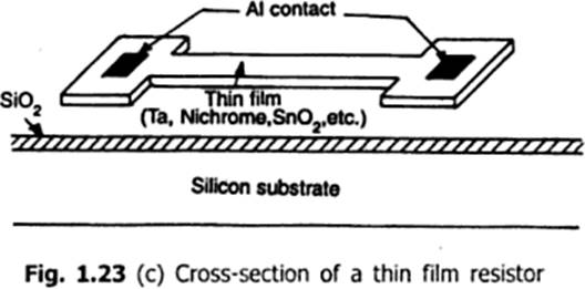
The thin film deposition technique can also be used for the fabrication of monolithic resistors. A very thin metallic film of thickness less than 1μm is deposited on the silicon dioxide layer by vapour deposition techniques. Normally, Nichrome (NiCr) is used for this process. Desired geometry is achieved using masked etching processes to obtain suitable value of resistors. Ohmic contacts are made using aluminium metallization as discussed in earlier sections.
The cross-sectional view of a thin film resistor as shown in figure. Sheet resistances of 40 to 400Ω/ square can be easily obtained in this method and thus 20kΩ to 50kΩ values are very practical.
The advantages of thin film resistors are as follows:
The thin film resistor can be obtained by the use of tantalum deposited over silicon dioxide layer. The main disadvantage of thin film resistor is that its fabrication requires additional processing steps.
Monolithic Capacitors:
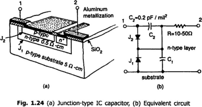
Monolithic capacitors are not frequently used in integrated circuits since they are limited in the range of values obtained and their performance. There are, however, two types available, the junction capacitor is a reverse biased PN junction formed by the collector-base or emitter-base diffusion of the transistor. The capacitance is proportional to the area of the junction and inversely proportional to the depletion thickness.
C α A, where a is the area of the junction and
C α T , where t is the thickness of the depletion layer.
The capacitance value thus obtainable can be around 1.2nF/mm2 .
The thin film or metal oxide silicon capacitor uses a thin layer of silicon dioxide as the dielectric. One plate is the connecting metal and the other is a heavily doped layer of silicon, which is formed during the emitter diffusion. This capacitor has a lower leakage current and is non- directional, since emitter plate can be biased positively. The capacitance value of this method can be varied between 0.3 and 0.8nF/mm2 .
Inductors:
No satisfactory integrated inductors exist. If high Q inductors with inductance of values larger than 5μH are required, they are usually supplied by a wound inductor which is connected externally to the chip. Therefore, the use of inductors is normally avoided when integrated circuits are used.
General Operational Amplifier:
An operational amplifier generally consists of three stages, anmely,1. a differential amplifier 2. additional amplifier stages to provide the required voltage gain and dc level shifting 3. an emitter-follower or source follower output stage to provide current gain and low output resistance.
A low-frequency or dc gain of approximately 104 is desired for a general purpose op-amp and hence, the use of active load is preferred in the internal circuitry of op-amp. The output voltage is required to be at ground, when the differential input voltages is zero, and this necessitates the use of dual polarity supply voltage. Since the output resistance of op-amp is required to be low, a complementary push-pull emitter – follower or source follower output stage is employed. Moreover, as the input bias currents are to be very small of the order of picoamperes, an FET input stage is normally preferred. The figure shows a general op-amp circuit using JFET input devices.
Input stage:
The input differential amplifier stage uses p-channel JFETs M1 and M2. It employs a three-transistor active load formed by Q3 , Q4 , and Q5 . the bias current for the stage is provided by a two-transistor current source using PNP transistors Q6 and Q7. Resistor R1 increases the output resistance seen looking into the collector of Q4 as indicated by R04. This is necessary to provide bias current stability against the transistor parameter variations. Resistor R2 establishes a definite bias current through Q5 . A single ended output is taken out at the collector of Q4 .
MOSFET’s are used in place of JFETs with additional devices in the circuit to prevent any damage for the gate oxide due to electrostatic discharges.
Gain stage:
The second stage or the gain stage uses Darlington transistor pair formed by Q8 and Q9 as shown in figure. The transistor Q8 is connected as an emitter follower, providing large input resistance.
Therefore, it minimizes the loading effect on the input differential amplifier stage. The transistor Q9 provides an additional gain and Q10 acts as an active load for this stage. The current mirror formed by Q7 and Q10 establishes the bias current for Q9 . The VBE drop across Q9 and drop across R5 constitute the voltage drop across R4 , and this voltage sets the current through Q8 . It can be set to a small value, such that the base current of Q8 also is very less.
Output stage:
The final stage of the op-amp is a class AB complementary push-pull output stage. Q11 is an emitter follower, providing a large input resistance for minimizing the loading effects on the gain stage. Bias current for Q11 is provided by the current mirror formed by Q7 and Q12, through Q13 and Q14 for minimizing the cross over distortion. Transistors can also be used in place of the two diodes.
The overall voltage gain AV of the op-amp is the product of voltage gain of each stage as given by AV = |Ad | |A2||A3|
Where Ad is the gain of the differential amplifier stage, A2 is the gain of the second gain stage and A3 is the gain of the output stage.
IC 741 Bipolar operational amplifier:
The IC 741 produced since 1966 by several manufactures is a widely used general purpose operational amplifier. Figure shows that equivalent circuit of the 741 op-amp, divided into various individual stages. The op-amp circuit consists of three stages.
A bias circuit is used to establish the bias current for whole of the circuit in the IC. The op-amp is supplied with positive and negative supply voltages of value ± 15V, and the supply voltages as low as ±5V can also be used.
Bias Circuit:
The reference bias current IREF for the 741 circuit is established by the bias circuit consisting of two diodes-connected transistors Q11 and Q12 and resistor R5. The widlar current source formed by Q11 , Q10 and R4 provide bias current for the differential amplifier stage at the collector of Q10. Transistors Q8 and Q9 form another current mirror providing bias current for the differential amplifier. The
reference bias current IREF also provides mirrored and proportional current at the collector of the double –collector lateral PNP transistor Q13. The transistor Q13 and Q12 thus form a two-output current mirror with Q13A providing bias current for output stage and Q13B providing bias current for Q17. The transistor Q18 and Q19 provide dc bias for the output stage. Formed by Q14 and Q20 and they establish two VBE drops of potential difference between the bases of Q14 and Q18 .
Input stage:
The input differential amplifier stage consists of transistors Q1 through Q7 with biasing provided by Q8 through Q12. The transistor Q1 and Q2 form emitter – followers contributing to high differential input resistance, and whose output currents are inputs to the common base amplifier using Q3 and Q4 which offers a large voltage gain.
The transistors Q5, Q6 and Q7 along with resistors R1, R2 and R3 from the active load for input stage. The single-ended output is available at the collector of Q6. the two null terminals in the input stage facilitate the null adjustment. The lateral PNP transistors Q3 and Q4 provide additional protection against voltage breakdown conditions. The emitter-base junction Q3 and Q4 have higher emitter-base breakdown voltages of about 50V. Therefore, placing PNP transistors in series with NPN transistors provide protection against accidental shorting of supply to the input terminals.
Gain Stage:
The Second or the gain stage consists of transistors Q16 and Q17, with Q16 acting as an emitter – follower for achieving high input resistance. The transistor Q17 operates in common emitter configuration with its collector voltage applied as input to the output stage. Level shifting is done for this signal at this stage.
Internal compensation through Miller compensation technique is achieved using the feedback capacitor C1 connected between the output and input terminals of the gain stage.
Output stage:
The output stage is a class AB circuit consisting of complementary emitter follower transistor pair Q14 and Q20 . Hence, they provide an effective loss output resistance and current gain.
The output of the gain stage is connected at the base of Q22 , which is connected as an emitter – follower providing a very high input resistance, and it offers no appreciable loading effect on the
gain stage. It is biased by transistor Q13A which also drives Q18 and Q19, that are used for establishing a quiescent bias current in the output transistors Q14 and Q20.
Ideal op-amp characteristics:
AC Characteristics:
For small signal sinusoidal (AC) application one has to know the ac characteristics such as frequency response and slew-rate.
Frequency Response:
The variation in operating frequency will cause variations in gain magnitude and its phase angle. The manner in which the gain of the op-amp responds to different frequencies is called the frequency response. Op-amp should have an infinite bandwidth Bw =∞ (i.e) if its open loop gain in 90dB with dc signal its gain should remain the same 90 dB through audio and onto high radio frequency. The op-amp gain decreases (roll-off) at higher frequency what reasons to decrease gain after a certain frequency reached. There must be a capacitive component in the equivalent circuit of the op-amp. For an op-amp with only one break (corner) frequency all the capacitors effects can be represented by a single capacitor C. Below fig is a modified variation of the low frequency model with capacitor C at the o/p.
Non-inverting Amplifier:
Figure shows the open – loop non- inverting amplifier. The input signal is applied to the non-inverting input terminal of the op-amp and the inverting input terminal is connected to the ground.
The input signal is amplified by the open – loop gain A and the output is in-phase with input signal.
V0 = AVi
In all the above open-loop configurations, only very small values of input voltages can be applied. Even for voltages levels slightly greater than zero, the output is driven into saturation, which is observed from the ideal transfer characteristics of op-amp shown in figure. Thus, when operated in the open-loop configuration, the output of the op-amp is either in negative or positive saturation, or switches between positive and negative saturation levels. This prevents the use of open – loop configuration of op-amps in linear applications.
Limitations of Open – loop Op – amp configuration:
Firstly, in the open – loop configurations, clipping of the output waveform can occur when the output voltage exceeds the saturation level of op-amp. This is due to the very high open – loop gain of the op-amp. This feature actually makes it possible to amplify very low frequency signal of the order of microvolt or even less, and the amplification can be achieved accurately without any
distortion. However, signals of such magnitudes are susceptible to noise and the amplification for those application is almost impossible to obtain in the laboratory.
Secondly, the open – loop gain of the op – amp is not a constant and it varies with changing temperature and variations in power supply. Also, the bandwidth of most of the open- loop op amps is negligibly small. This makes the open – loop configuration of op-amp unsuitable for ac applications. The open – loop bandwidth of the widely used 741 IC is approximately 5Hz. But in almost all ac applications, the bandwidth requirement is much larger than this.
For the reason stated, the open – loop op-amp is generally not used in linear applications. However, the open – loop op amp configurations find use in certain non – linear applications such as comparators, square wave generators and astable multivibrators.
Closed – loop op-amp configuration:
The op-amp can be effectively utilized in linear applications by providing a feedback from the output to the input, either directly or through another network. If the signal feedback is out- of- phase by 1800 with respect to the input, then the feedback is referred to as negative feedback or degenerative feedback. Conversely, if the feedback signal is in phase with that at the input, then the feedback is referred to as positive feedback or regenerative feedback.
An op – amp that uses feedback is called a closed – loop amplifier. The most commonly used closed – loop amplifier configurations are 1. Inverting amplifier (Voltage shunt amplifier) 2. Non- Inverting amplifier (Voltage – series Amplifier)
Inverting Amplifier:
The inverting amplifier is shown in figure and its alternate circuit arrangement is shown in figure, with the circuit redrawn in a different way to illustrate how the voltage shunt feedback is achieved. The input signal drives the inverting input of the op – amp through resistor R1 .
The op – amp has an open – loop gain of A, so that the output signal is much larger than the error voltage. Because of the phase inversion, the output signal is 1800 out – of – phase with the input signal. This means that the feedback signal opposes the input signal and the feedback is negative or degenerative.
Types of ADC
Direct-conversion ADC/Flash type ADC:
This process is extremely fast with a sampling rate of up to 1 GHz. The resolution is however, limited because of the large number of comparators and reference voltages required. The input signal is fed simultaneously to all comparators. A priority encoder then generates a digital output that corresponds with the highest activated comparator.
Successive-approximationADCs
Successive-approximation ADC is a conversion technique based on a successive-approximation register (SAR). This is also called bit-weighing conversion that employs a comparator to weigh the applied input voltage against the output of an N-bit digital-to-analog converter (DAC). The final
result is obtained as a sum of N weighting steps, in which each step is a single-bit conversion using the DAC output as a reference. SAR converters sample at rates up to 1Mbps, requires a low supply current, and the cheapest in terms of production cost.
A successive-approximation ADC uses a comparator to reject ranges of voltages, eventually settling on a final voltage range. Successive approximation works by constantly comparing the input voltage to the output of an internal digital to analog converter (DAC, fed by the current value of the approximation) until the best approximation is achieved. At each step in this process, a binary value of the approximation is stored in a successive approximation register (SAR). The SAR uses a reference voltage (which is the largest signal the ADC is to convert) for comparisons. For example if the input voltage is 60 V and the reference voltage is 100 V, in the 1st clock cycle, 60 V is compared to 50 V (the reference, divided by two. This is the voltage at the output of the internal DAC when the input is a '1' followed by zeros), and the voltage from the comparator is positive (or '1') (because 60 V is greater than 50 V). At this point the first binary digit (MSB) is set to a '1'. In the 2nd clock cycle the input voltage is compared to 75 V (being halfway between 100 and 50 V: This is the output of the internal DAC when its input is '11' followed by zeros) because 60 V is less than 75 V, the comparator output is now negative (or '0'). The second binary digit is therefore set to a '0'. In the 3rd clock cycle, the input voltage is compared with 62.5 V (halfway between 50 V and 75 V: This is the output of the internal DAC when its input is '101' followed by zeros). The output of the comparator is negative or '0' (because 60 V is less than 62.5 V) so the third binary digit is set to a 0. The fourth clock cycle similarly results in the fourth digit being a '1' (60 V is greater than 56.25 V, the DAC output for '1001' followed by zeros). The result of this would be in the binary form 1001. This is also called bit-weighting conversion, and is similar to a binary. The analogue value is rounded to the nearest binary value below, meaning this converter type is mid-rise (see above). Because the approximations are successive (not simultaneous), the conversion takes one clock-cycle for each bit of resolution desired. The clock frequency must be equal to the sampling frequency multiplied by the number of bits of resolution desired. For example, to sample audio at 44.1 kHz with 32 bit resolution, a clock frequency of over 1.4 MHz would be required. ADCs of this type have good resolutions and quite wide ranges. They are more complex than some other designs.
IntegratingADCs
In an integrating ADC, a current, proportional to the input voltage, charges a capacitor for a fixed time interval T charge. At the end of this interval, the device resets its counter and applies an opposite-polarity negative reference voltage to the integrator input. Because of this, the capacitor is discharged by a constant current until the integrator output voltage zero again. The T discharge interval is proportional to the input voltage level and the resultant final count provides the digital output, corresponding to the input signal. This type of ADCs is extremely slow devices with low input bandwidths. Their advantage, however, is their ability to reject high-frequency noise and AC line noise such as 50Hz or 60Hz. This makes them useful in noisy industrial environments and typical application is in multi-meters.
An integrating ADC (also dual-slope or multi-slope ADC) applies the unknown input voltage to the input of an integrator and allows the voltage to ramp for a fixed time period (the run-up period). Then a known reference voltage of opposite polarity is applied to the integrator and is allowed to ramp until the integrator output returns to zero (the run-down period). The input voltage is computed as a function of the reference voltage, the constant run-up time period, and the measured run-down time period. The run-down time measurement is usually made in units of the converter's clock, so longer integration times allow for higher resolutions. Likewise, the speed of the converter can be improved by sacrificing resolution. Converters of this type (or variations on the concept) are used in most digital voltmeters for their linearity and flexibility.

Sigma-delta ADCs/ Over sampling Converters:
It consist of 2 main parts - modulator and digital filter. The modulator includes an integrator and a comparator with a feedback loop that contains a 1-bit DAC. The modulator oversamples the input signal, converting it to a serial bit stream with a frequency much higher than the required sampling rate. This is then transform by the output filter to a sequence of parallel digital words at the sampling rate. The characteristics of sigma-delta converters are high resolution, high accuracy, low noise and low cost. Typical applications are for speech and audio.
A Sigma-Delta ADC (also known as a Delta-Sigma ADC) oversamples the desired signal by a large factor and filters the desired signal band. Generally a smaller number of bits than required are converted using a Flash ADC after the Filter. The resulting signal, along with the error generated by the discrete levels of the Flash, is fed back and subtracted from the input to the filter. This negative feedback has the effect of noise shaping the error due to the Flash so that it does not appear in the desired signal frequencies. A digital filter (decimation filter) follows the ADC which reduces the sampling rate, filters off unwanted noise signal and increases the resolution of the output. (sigma-delta modulation, also called delta-sigma modulation)
A/D Using Voltage to time conversion:
The Block diagram shows the basic voltage to time conversion type of A to D converter. Here the cycles of variable frequency source are counted for a fixed period. It is possible to make an A/D converter by counting the cycles of a fixed-frequency source for a variable period. For this, the analog voltage required to be converted to a proportional time period.
As shown in the diagram, A negative reference voltage -VR is applied to an integrator, whose output is connected to the inverting input of the comparator. The output of the comparator is at 1 as long as the output of the integrator Vo is less than Va. At t = T, Vc goes low and switch S remains open. When VEN goes high, the switch S is closed, thereby discharging the capacitor. Also the NAND gate is disabled. The waveforms are shown here.
SWITCHING REGULATORS
Introduction
The switching regulator is increasing in popularity because it offers the advantages of higher power conversion efficiency and increased design flexibility (multiple output voltages of different polarities can be generated from a single input voltage).
Although most power supplies used in amateur shacks are of the linear regulator type, an increasing number of switching power supplies have become available to the amateur. For most amateurs the switching regulator is still somewhat of a mystery. One might wonder why we even bother with these power supplies, when the existing linear types work just fine. The primary advantage of a switching regulator is very high efficiency, a lot less heat and smaller size. To understand how these black boxes work lets take a look at a traditional linear regulator at right. As we see in the diagram, the linear regulator is really nothing more than a variable resistor. The resistance of the regulator varies in accordance with the load resulting in a constant output voltage
The primary filter capacitor is placed on the input to the regulator to help filter out the 60 cycle ripple. The linear regulator does an excellent job but not without cost. For example, if the output voltage is 12 volts and the input voltage is 24 volts then we must drop 12 volts across the regulator. At output currents of 10 amps this translates into 120 watts (12 volts times 10 amps) of heat energy that the regulator must dissipate. Is it any wonder why we have to use those massive heat sinks? As we can see this results in a mere 50% efficiency for the linear regulator and a lot of wasted power which is normally transformed into heat.
The time that the switch remains closed during each switch cycle is varied to maintain a constant output voltage. Notice that the primary filter capacitor is on the output of the regulator and not the input. As is apparent, the switching regulator is much more efficient than the linear regulator achieving efficiencies as high as 80% to 95% in some circuits. The obvious result is smaller heat sinks, less heat and smaller overall size of the power supply.
The previous diagram is really an over simplification of a switching regulator circuit. An actual switching regulator circuit more closely resembles the circuit below: Now lets take a look at a very basic switching regulator at right. As we see can see, the switching regulator is really nothing more than just a simple switch. This switch goes on and off at a fixed rate usually between 50Khz to 100Khz as set by the circuit.
As we see above the switching regulator appears to have a few more components than a linear regulator. Diode D1 and Inductor L1 play a very specific role in this circuit and are found in almost every switching regulator. First, diode D1 has to be a Schottky or other very fast switching diode. A 1N4001 just won't switch fast enough in this circuit. Inductor L1 must be a type of core that does not saturate under high currents. Capacitor C1 is normally a low ESR (Equivalent Series Resistance) type.
To understand the action of D1 and L1, lets look at what happens when S1 is closed as indicated below:
As we see above, L1, which tends to oppose the rising current, begins to generate an electromagnetic field in its core. Notice that diode D1 is reversed biased and is essentially an open circuit at this point. Now lets take a look at what happens when S1 opens below:
As we see in this diagram the electromagnetic field that was built up in L1 is now discharging and generating a current in the reverse polarity. As a result, D1 is now
conducting and will continue until the field in L1 is diminished. This action is similar to the charging and discharging of capacitor C1. The use of this inductor/diode combination gives us even more efficiency and augments the filtering of C1.
Because of the unique nature of switching regulators, very special design considerations are required. Because the switching system operates in the 50 to 100 kHz region and has an almost square waveform, it is rich in harmonics way up into the HF and even the VHF/UHF region. Special filtering is required, along with shielding, minimized lead lengths and all sorts of toroidal filters on leads going outside the case. The switching regulator also has a minimum load requirement, which is determined by the inductor value. Without the minimum load, the regulator will generate excessive noise and harmonics and could even damage itself. (This is why it is not a good idea to turn on a computer switching power supply without some type of load connected.) To meet this requirement, many designers use a cooling fan and or a minimum load which switches out when no longer needed.
Fortunately, recent switching regulator IC's address most of these design problems quite well. Because of lowered component costs as well as a better understanding of switching regulator technology, we are starting to see even more switching power supplies replacing traditionally linear only applications. It is no doubt that we will see fewer linear power supplies being used in the future.
In this article we addressed basic switching regulator design concepts and it is hoped that amateurs will begin to look at switching regulators much more seriously when they decide to replace an old power supply. In a future construction article, we will review an actual switching regulator circuit.
IC VOLTAGE REGULATORS
Four most commonly used switching converter types:
Buck: used the reduce a DC voltage to a lower DC voltage. Boost: provides an output voltage that is higher than the input.
Buck-Boost (invert): an output voltage is generated opposite in polarity to the input.
Flyback: an output voltage that is less than or greater than the input can be generated, as well as multiple outputs.
Converters:
Push-Pull: A two-transistor converter that is especially efficient at low input voltages. Half-Bridge: A two-transistor converter used in many off-line applications.
Full-Bridge: A four-transistor converter (usually used in off-line designs) that can
generate the highest output power of all the types listed.
Application information will be provided along with circuit examples that illustrate some applications of Buck, Boost, and Flyback regulators.
Switching Fundamentals The law of inductance
If a voltage is forced across an inductor, a current will flow through that inductor (and
this current will vary with time). The current flowing in an inductor will be time-varying even if the forcing voltage is constant. It is equally correct to say that if a time-varying current is forced to flow in an inductor, a voltage across the inductor will result. The fundamental law that defines the relationship between the voltage and current in an inductor is given by the equation:
v = L (di/dt)
Two important characteristics of an inductor that follow directly from the law of inductance are:
Flyback Regulator:
The Flyback is the most versatile of all the topologies, allowing the designer to create one or more output voltages, some of which may be opposite in polarity. Flyback converters have gained popularity in battery-powered systems, where a single voltage must be converted into the required system voltages (for example, +5V, +12V and -12V) with very high power conversion efficiency. The basic single-output flyback converter is shown in Figure.
The most important feature of the Flyback regulator is the transformer phasing, as shown by the dots on the primary and secondary windings. When the switch is on, the input voltage is forced across the transformer primary which causes an increasing flow of current through it. Note that the polarity of the voltage on the primary is dot-negative (more negative at the dotted end), causing a voltage with the same polarity to appear at the transformer secondary (the magnitude of the secondary voltage is set by the transformer seconday-to-primary turns ratio).
The dot-negative voltage appearing across the secondary winding turns off the diode, reventing current flow in the secondary winding during the switch on time. During this time, the load current must be supplied by the output capacitor alone. When the switch turns off, the decreasing current flow in the primary causes the voltage at the dot end to swing positive. At the same time, the primary voltage is reflected to the secondary with the same polarity. The dot-positive voltage occurring across the secondary winding turns on the diode, allowing current to flow into both the load and the output capacitor. The output capacitor charge lost to the load during the switch on time is replenished during the switch off time. Flyback converters operate in either continuous mode (where the secondarycurrent is always >0) or discontinuous mode (where the secondary current falls to zero on each cycle).
Generating Multiple Outputs:
Another big advantage of a Flyback is the capability of providing multiple outputs .In such applications, one of the outputs (usually the highest current) is selected to provide PWM feedback to the control loop, which means this output is directly regulated. The other secondary winding(s) are indirectly regulated, as their pulse widths will follow the regulated winding. The load regulation on the unregulated secondaries is not great (typically 5 - 10%), but is adequate for many applications.
If tighter regulation is needed on the lower current secondaries, an LDO post-regulator is an excellent solution. The secondary voltage is set about 1V above the desired output voltage, and the LDO provides excellent output regulation withvery little loss of efficiency.
The Push-Pull converter uses two to transistors perform DC-DC conversion.The converter operates by turning on each transistor on alternate cycles (the two transistors are never on at the same time). Transformer secondary current flows at the same time as primary current (when either of the switches is on). For example, when transistor "A" is turned on, the input voltage is forced across the upper primary winding with dot-negative polarity. On the secondary side, a dot-negative voltage will appear across the winding which turns on the bottom diode.This allows current to flow into the inductor to supply both the output capacitor and the load. When transistor "B" is on, the input voltage is forced across the lower primary winding with dot-positive polarity.
The same voltage polarity on the secondary turns on the top diode, and current flows into the output capacitor and the load. An important characteristic of a Push-Pull converter is that the switch transistors have to be able the stand off more than twice the input voltage: when one transistor is on (and the input voltage is forced across one primary winding) the same magnitude voltage is induced across the other primary winding, but it is "floating" on top of the input voltage. This puts the collector of the turned-off transistor at twice the input voltage with respect to ground. The "double input voltage" rating requirement of the switch transistors means the Push-Pull converter is best suited for lower input voltage applications. It has been widely used in converters operating in 12V and 24V battery-powered systems.
Figure shows a timing diagram which details the relationship of the input and output pulses. It is important to note that frequency of the secondary side voltage pulses is twice the frequency of
operation of the PWM controller driving the two transistors. For example, if the PWM control chip was set up to operate at 50 kHz on the primary
side, the frequency of the secondary pulses would be 100 kHz.
This highlights why the Push-Pull converter is well-suited for low voltage converters.
The voltage forced across each primary winding (which provides the power for conversion) is the full input voltage minus only the saturation voltage of the switch. If MOS-FET power switches are used, the voltage drop across the switches can be made extremely small, resulting in very high utilization of the available input voltage. Another advantage of the Push-Pull converter is that it can also generate multiple output voltages (by adding more secondary windings), some of which may be negative in polarity. This allows a power supply operated from a single battery to provide all of the voltages necessary for system operation.
A disadvantage of Push-Pull converters is that they require very good matching of the switch transistors to prevent unequal on times, since this will result in saturation of the transformer core (and failure of the converter).
Output Capacitor ESR effects:
The primary function of the output capacitor in a switching regulator is filtering. As the converter operates, current must flow into and out of the output filter capacitor. The ESR of the output capacitor directly affects the performance of the switching regulator. ESR is specified by the manufacturer on good quality capacitors, but be certain that it is specified at the frequency of intended operation.
General-purpose electrolytes usually only specify ESR at 120 Hz, but capacitors intended for high- frequency switching applications will have the ESR guaranteed at high frequency (like 20 kHz to 100 kHz). Some ESR dependent parameters are: Ripple Voltage: In most cases, the majority of the output ripples voltage results from the ESR of the output capacitor. If the ESR increases (as it will at low operating temperatures) the output ripple voltage will increase accordingly.
Efficiency: As the switching current flows into and out of the capacitor (through the ESR), power is dissipated internally. This "wasted" power reduces overall regulator efficiency, and can also cause the capacitor to fail if the ripple current exceeds the maximum allowable specification for the capacitor.
Loop Stability: The ESR of the output capacitor can affect regulator loop stability. Products such as the LM2575 and LM2577 are compensated for stability assumingthe ESR of the output capacitor will stay within a specified range. Keeping the ESR within the "stable" range is not always simple in designs that must operate over a wide temperature range. The ESR of a typical aluminum electrolytic may increase by 40X as the temperature drops from 25°C to -40°C.
In these cases, an aluminum electrolytic must be paralleled by another type ofcapacitor with a flatter ESR curve (like Tantalum or Film) so that the effective ESR (which is the parallel value of the two ESR's) stays within the allowable range. Note: if operation below -40°C is necessary, aluminum electrolytics are probably not feasible for use.
Bypass Capacitors:
High-frequency bypass capacitors are always recommended on the supply pins of IC devices, but if the devices are used in assemblies near switching converters bypass capacitors are absolutely required. The components which perform the high-speed switching (transistors and rectifiers) generate significant EMI that easily radiates into PC board traces and wire leads. To assure proper circuit operation, all IC supply pins must be bypassed to a clean, low-inductance ground.
Proper Grounding:
The "ground" in a circuit is supposed to be at one potential, but in real life it is not.
When ground currents flow through traces which have non-zero resistance, voltage
differences will result at different points along the ground path. In DC or low-frequency circuits, "ground management" is comparatively simple: the only parameter of critical importance is the DC resistance of a conductor, since that defines the voltage drop across it for a given current. In high-frequency circuits, it is the inductance of a trace or conductor that is much more important.
In switching converters, peak currents flow in high-frequency (> 50 kHz) pulses, which can cause severe problems if trace inductance is high. Much of the "ringing" and "spiking" seen on voltage waveforms in switching converters is the result of high current being switched through parasitic trace (or wire) inductance.Current switching at high frequencies tends to flow near the surface of a conductor (this is called "skin effect"), which means that ground traces must be very wide on a PC board to avoid problems. It is usually best (when possible) to use one side of the PC board as a ground plane. The following diagram shows the poor grounding.

The layout shown has the high-power switch return current passing through a trace that also provides the return for the PWM chip and the logic circuits. The switching current pulses flowing through the trace will cause a voltage spike (positive and negative) to occur as a result of the rising and falling edge of the switch current. This voltage spike follows directly from the v = L (di/dt) law of inductance. It is important to note that the magnitude of the spike will be different at all points along the trace, being largest near the power switch. Taking the ground symbol as a point of reference, this shows how all three circuits would be bouncing up and down with respect to ground. More important, they would also be moving with respect to each other.
Mis-operation often occurs when sensitive parts of the circuit "rattle" up and down due to ground switching currents. This can induce noise into the reference used to set the output voltage, resulting in excessive output ripple. Very often, regulators that suffer from ground noise problems appear to be unstable, and break into oscillations as the load current is increased (which increases ground currents). The figure shows good grounding.
Source: http://fmcet.in/ECE/EC2254_uw.pdf
Web site to visit: http://fmcet.in
Author of the text: indicated on the source document of the above text
If you are the author of the text above and you not agree to share your knowledge for teaching, research, scholarship (for fair use as indicated in the United States copyrigh low) please send us an e-mail and we will remove your text quickly. Fair use is a limitation and exception to the exclusive right granted by copyright law to the author of a creative work. In United States copyright law, fair use is a doctrine that permits limited use of copyrighted material without acquiring permission from the rights holders. Examples of fair use include commentary, search engines, criticism, news reporting, research, teaching, library archiving and scholarship. It provides for the legal, unlicensed citation or incorporation of copyrighted material in another author's work under a four-factor balancing test. (source: http://en.wikipedia.org/wiki/Fair_use)
The information of medicine and health contained in the site are of a general nature and purpose which is purely informative and for this reason may not replace in any case, the council of a doctor or a qualified entity legally to the profession.
The texts are the property of their respective authors and we thank them for giving us the opportunity to share for free to students, teachers and users of the Web their texts will used only for illustrative educational and scientific purposes only.
All the information in our site are given for nonprofit educational purposes